- 您现在的位置:买卖IC网 > Sheet目录1214 > EVAL-ADUMQSEBZ (Analog Devices Inc)EVAL BOARD FOR ICOUPLER SMD
�� ��
��
��Evaluation� Board� User� Guide�
�EVALUATION� BOARD� HARDWARE�
�PAD� LAYOUT� FOR� THE� DUT�
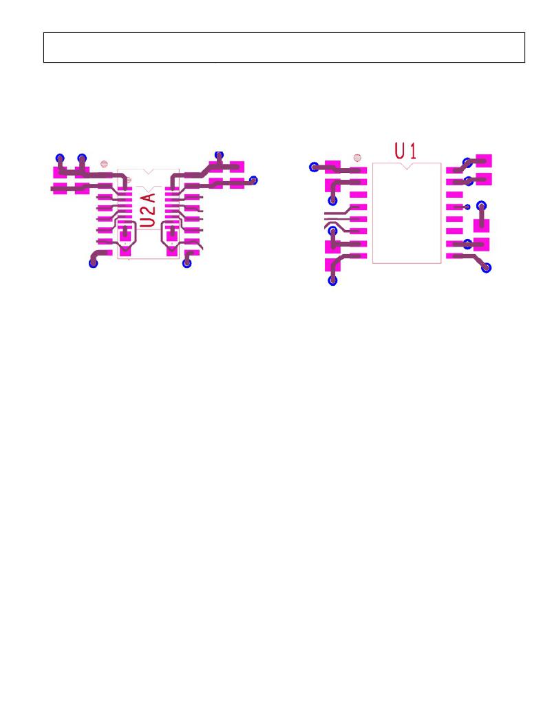
�The� evaluation� board� has� a� pad� layout� in� U2� that� accommo-�
�dates� 16-lead,� wide-body� SOIC� devices,� as� well� as� QSOP�
�miniature� packages,� as� shown� in� Figure� 2.� Power� and� ground�
�connections� connect� to� capacitor� pads� for� Side� 1� and� Side� 2.�
�Figure� 2.� DUT� Pad� Layout� Component� U2�
�Three� low� inductance,� surface-mount� bypass� capacitors� are�
�provided� for� each� side.� A� 100� nF� capacitor� is� installed� on� each�
�side� in� Capacitor� C2� and� Capacitor� C3.� Additional� bypass�
�capacitors� required� for� QSOP� packages� are� below� the� QSOP�
�pads� and� within� the� pad� layout� of� the� SOIC� package.� They�
�cannot� be� installed� if� the� SOIC� is� used.�
�In� addition,� there� are� 10� μF� ceramic� X7R� capacitors,� C1� on� Side� 1�
�and� C4� on� Side� 2,� that� provide� high� frequency� bypassing� and�
�ripple� reduction.� For� further� ripple� reduction� in� iso� Power?�
�devices� like� the� ADuM540x,� tantalum� capacitors� are� added� to�
�C10� as� a� 68� μF� value� on� Side� 1� and� to� C5� as� a� 22� μF� value� on�
�Side� 2.� These� large� value� ceramic� and� tantalum� bypass� capacitors�
�are� not� necessary� for� non-� iso� Power� devices.�
�Many� of� the� i� Coupler� devices� have� configuration� pins� that� allow�
�outputs� to� be� disabled� or� default� levels� to� be� set.� These� pins� are�
�usually� located� at� Pin� 7� and� Pin� 10� in� the� wide-body� package.� Pull-�
�up� 0� Ω� resistors� on� SM� Pad� R4� and� SM� Pad� R17� are� provided� to�
�pull� these� pins� high.� These� pull-up� resistors� can� be� removed,�
�and� pull-down� resistors� can� be� installed� on� R5� and� R18.�
�In� addition� to� the� U2� DUT� space,� an� additional� pad� layout� is�
�provided� at� U1,� specifically� to� accommodate� an� ADuM5000�
�iso� Power� device,� as� shown� in� Figure� 3.� This� is� a� power� supply�
�only� device� that� can� be� used� to� provide� secondary� power� for�
�any� i� Coupler� in� standalone� mode� or� as� a� slave� to� boost� power� to�
�the� ADuM520x� or� ADuM540x� devices.� The� surface-mount�
�resistor� pads� that� are� used� to� control� these� functions� are� not�
�populated.�
�An� ADuM5000� is� not� installed� at� Position� U1;� it� is� left� to� the�
�user� to� obtain� and� install� this� device� if� required.� As� shown� in�
�Figure� 3,� the� power� and� ground� connections� for� this� device� are�
�different� from� the� rest� of� the� i� Coupler� components.� The� C6� to�
�C9� pad� positions� for� bypass� capacitors� are� provided� but� not�
�UG-042�
�Pull-up,� pull-down,� and� connecting� resistor� pads� are� provided�
�(but� not� populated)� to� connect� the� ADuM5000� in� master� or� slave�
�mode,� as� well� as� to� set� the� output� voltage.� See� the� ADuM5000�
�data� sheet� for� descriptions� of� the� pin� functions.�
�Figure� 3.� ADuM5000� Pad� Layout� Component� U1�
�Grounding� Scheme�
�The� board� consists� of� two� separate� ground� and� power� systems.�
�Each� side� of� the� DUT� can� be� operated� from� an� independent�
�power� and� ground� reference.� This� allows� simulation� of�
�conditions� similar� to� the� target� application.� The� board� provides�
�for� board� creepage� and� clearance� typical� of� most� 2.5� kV� circuit�
�boards.� It� is� not� recommended� for� use� above� 2.5� kV� rms� transient�
�voltages� or� for� isolation� voltage� testing� above� 2500� V� rms.�
�EMI� and� EMC� Measurements�
�The� signal� path� has� been� made� as� simple� as� possible� while� still�
�providing� flexibility.� The� board� is� not� intended� for� detailed�
�characterization� of� system� noise,� EMI,� or� EMC.� It� may� be� useful�
�for� initial� bench� work� in� these� areas,� but� Analog� Devices,� Inc.,�
�does� not� guarantee� that� board� results� will� be� indicative� of� the�
�final� system� performance� in� these� areas.� The� board� includes�
�some� of� the� structures� discussed� in� the� AN-0971� Application�
�Note� for� radiated� EMI� mitigation.�
�TERMINALS�
�Side� 1� Power� Supply� Inputs�
�Power� is� supplied� to� the� board� via� a� set� of� terminal� block�
�connectors� labeled� IO_1C,� as� shown� in� Figure� 4.� Power� is�
�connected� to� the� Pin� 1� top� terminal,� and� ground� is� connected� to�
�the� Pin� 2� top� terminal.� Provisions� for� adding� in-line� inductors�
�for� noise� isolation� have� been� made� with� the� inclusion� of� Z1� and�
�Z2,� which� are� 1206� size� surface-mount� components.� These�
�positions� are� populated� with� 0� Ω� resistors� to� connect� power� to�
�the� board.� If� ferrite� inductors� are� required� for� noise� control,�
�these� components� should� be� removed� and� replaced� with�
�appropriate� inductors.�
�populated� (0.1� μF� X7R� ceramic� capacitors� are� recommended).�
�Rev.� A� |� Page� 3� of� 8�
�发布紧急采购,3分钟左右您将得到回复。
相关PDF资料
EVAL-ADUSB2EBUZ
BOARD EVAL USBI
EVAL-ADV7195EB
BOARD EVAL FOR ADV7195
EVAL-ADV7401EBZ
BOARD EVALUATION FOR ADV7401
EVAL-ADV7403EBZ
BOARD EVALUATION FOR ADV7403
EVAL-ADV7510P-ABZ
BOARD EVAL FOR ADV7510
EVAL-ADV7800EB1Z
BOARD EVAL EXTERNAL DDR SD MEM
EVAL-ADV7802EB1Z
BOARD EVAL EXTERNAL DDR SD MEM
EVAL-ADV7840EB1Z
BOARD EVAL FOR ADV7840
相关代理商/技术参数
EVAL-ADUSB1EBZ
制造商:Analog Devices 功能描述:USB TO SPI/12C CONVERTER - Boxed Product (Development Kits)
EVAL-ADUSB2EBUZ
功能描述:BOARD EVAL USBI RoHS:是 类别:编程器,开发系统 >> 配件 系列:SigmaDSP® 产品培训模块:Lead (SnPb) Finish for COTS
Obsolescence Mitigation Program RoHS指令信息:IButton RoHS Compliance Plan 标准包装:1 系列:- 附件类型:USB 至 1-Wire? RJ11 适配器 适用于相关产品:1-Wire? 设备 产品目录页面:1429 (CN2011-ZH PDF)
EVAL-ADUSB2EBZ
功能描述:BOARD EVAL USB TO SPI/12C RoHS:是 类别:编程器,开发系统 >> 配件 系列:SigmaDSP® 标准包装:1 系列:- 附件类型:适配器板 适用于相关产品:RCB230,RCB231,RCB212 配用:26790D-ND - RCB BREAKOUT BOARD RS232 CABLE
EVAL-ADV3014EBZ
功能描述:BOARD EVALUATION FOR ADV3014 RoHS:是 类别:编程器,开发系统 >> 评估演示板和套件 系列:- 标准包装:1 系列:PCI Express® (PCIe) 主要目的:接口,收发器,PCI Express 嵌入式:- 已用 IC / 零件:DS80PCI800 主要属性:- 次要属性:- 已供物品:板
EVAL-ADV7170EBM
制造商:AD 制造商全称:Analog Devices 功能描述:Digital PAL/NTSC Video Encoder
EVAL-ADV7171EBM
制造商:Analog Devices 功能描述:EVALUATION BOARD FOR DIGITAL PAL/NTSC VIDEO ENCODER WITH 10-BIT SSAF AND ADVANCED POWER MANAGEMENT
EVAL-ADV7173EBM
制造商:Analog Devices 功能描述:EVALUATION CONTROL BOARD I.C. - Bulk
EVAL-ADV7173EBZ
功能描述:BOARD EVALUATION FOR ADV7173 RoHS:是 类别:编程器,开发系统 >> 评估演示板和套件 系列:Advantiv® 标准包装:1 系列:- 主要目的:电信,线路接口单元(LIU) 嵌入式:- 已用 IC / 零件:IDT82V2081 主要属性:T1/J1/E1 LIU 次要属性:- 已供物品:板,电源,线缆,CD 其它名称:82EBV2081